- 您现在的位置:买卖IC网 > Sheet目录2004 > LTC1750IFW#PBF (Linear Technology)IC ADC 14BIT 80MSPS SMPL 48TSSOP
17
LTC1750
1750f
APPLICATIO S I FOR ATIO
WU
UU
Output Loading
As with all high speed/high resolution converters the
digital output loading can affect the performance. The
digital outputs of the LTC1750 should drive a minimal
capacitive load to avoid possible interaction between the
digital outputs and sensitive input circuitry. The output
should be buffered with a device such as an ALVCH16373
CMOS latch. For full speed operation the capacitive load
should be kept under 10pF. A resistor in series with the
output may be used but is not required since the ADC has
a series resistor of 43
on chip.
Lower OVDD voltages will also help reduce interference
from the digital outputs.
Format
The LTC1750 parallel digital output can be selected for
offset binary or 2’s complement format. The format is
selected with the MSBINV pin; high selects offset binary.
Overflow Bit
An overflow output bit indicates when the converter is
overranged or underranged. When OF outputs a logic high
the converter is either overranged or underranged.
Output Clock
The ADC has a delayed version of the ENC input available
as a digital output, CLKOUT. The CLKOUT pin can be used
to synchronize the converter data to the digital system.
This is necessary when using a sinusoidal encode signal.
Data will be updated just after CLKOUT falls and can be
latched on the rising edge of CLKOUT.
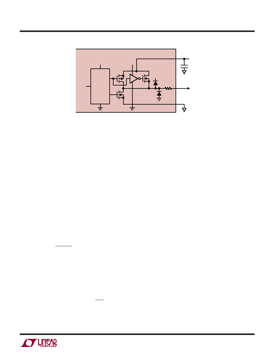
Output Driver Power
Separate output power and ground pins allow the output
drivers to be isolated from the analog circuitry. The power
supply for the digital output buffers, OVDD, should be tied
to the same power supply as for the logic being driven. For
example if the converter is driving a DSP powered by a 3V
supply then OVDD should be tied to that same 3V supply.
OVDD can be powered with any voltage up to 5V. The logic
outputs will swing between OGND and OVDD.
GROUNDING AND BYPASSING
The LTC1750 requires a printed circuit board with a clean
unbroken ground plane. A multilayer board with an inter-
nal ground plane is recommended. The pinout of the
LTC1750 has been optimized for a flowthrough layout so
that the interaction between inputs and digital outputs is
minimized. Layout for the printed circuit board should
ensure that digital and analog signal lines are separated as
much as possible. In particular, care should be taken not
to run any digital track alongside an analog signal track or
underneath the ADC.
High quality ceramic bypass capacitors should be used at
the VDD, VCM, REFHA, REFHB, REFLA and REFLB pins as
shown in the block diagram on the front page of this data
sheet. Bypass capacitors must be located as close to the
pins as possible. Of particular importance are the capaci-
tors between REFHA and REFLB and between REFHB and
LTC1750
1750 F09
OVDD
VDD
0.1
F
43
TYPICAL
DATA
OUTPUT
OGND
OVDD
0.5V TO
VDD
PREDRIVER
LOGIC
DATA
FROM
LATCH
Figure 9. Equivalent Circuit for a Digital Output Buffer
发布紧急采购,3分钟左右您将得到回复。
相关PDF资料
LTC1799HS5#TRPBF
IC OSC SILICON 33MHZ TSOT23-5
LTC1821ACGW
IC D/A CONV 16BIT PRECISE 36SSOP
LTC1851CFW
IC ADC 12BIT 1.25MSPS 48-TSSOP
LTC1853IFW#TRPBF
IC A/D CONV 8CH 12BIT 48-TSSOP
LTC1856IG#PBF
IC ADC 16BIT 100KSPS 28-SSOP
LTC1859IG#TRPBF
IC A/D CONV 8CH 16BIT 28-SSOP
LTC1867AIGN#TRPBF
IC ADC 16BIT 8CH 200KSPS 16SSOP
LTC1867LCGN#PBF
IC ADC 16BIT 8CH 175KSPS 16SSOP
相关代理商/技术参数
LTC1750IFW#TR
功能描述:IC ADC 14BIT 80MSPS SMPL 48TSSOP RoHS:否 类别:集成电路 (IC) >> 数据采集 - 模数转换器 系列:- 标准包装:1 系列:- 位数:14 采样率(每秒):83k 数据接口:串行,并联 转换器数目:1 功率耗散(最大):95mW 电压电源:双 ± 工作温度:0°C ~ 70°C 安装类型:通孔 封装/外壳:28-DIP(0.600",15.24mm) 供应商设备封装:28-PDIP 包装:管件 输入数目和类型:1 个单端,双极
LTC1750IFW#TRPBF
功能描述:IC ADC 14BIT 80MSPS SMPL 48TSSOP RoHS:是 类别:集成电路 (IC) >> 数据采集 - 模数转换器 系列:- 产品培训模块:Lead (SnPb) Finish for COTS
Obsolescence Mitigation Program 标准包装:2,500 系列:- 位数:12 采样率(每秒):3M 数据接口:- 转换器数目:- 功率耗散(最大):- 电压电源:- 工作温度:- 安装类型:表面贴装 封装/外壳:SOT-23-6 供应商设备封装:SOT-23-6 包装:带卷 (TR) 输入数目和类型:-
LTC1751EMS8
功能描述:IC REG SWITCHD CAP DBL ADJ 8MSOP RoHS:否 类别:集成电路 (IC) >> PMIC - 稳压器 - DC DC 开关稳压器 系列:- 标准包装:2,500 系列:- 类型:升压(升压) 输出类型:可调式 输出数:1 输出电压:1.24 V ~ 30 V 输入电压:1.5 V ~ 12 V PWM 型:电流模式,混合 频率 - 开关:600kHz 电流 - 输出:500mA 同步整流器:无 工作温度:-40°C ~ 85°C 安装类型:表面贴装 封装/外壳:8-SOIC(0.154",3.90mm 宽) 包装:带卷 (TR) 供应商设备封装:8-SOIC
LTC1751EMS8#PBF
功能描述:IC REG SWITCHD CAP DBL ADJ 8MSOP RoHS:是 类别:集成电路 (IC) >> PMIC - 稳压器 - DC DC 开关稳压器 系列:- 标准包装:250 系列:- 类型:降压(降压) 输出类型:固定 输出数:1 输出电压:1.2V 输入电压:2.05 V ~ 6 V PWM 型:电压模式 频率 - 开关:2MHz 电流 - 输出:500mA 同步整流器:是 工作温度:-40°C ~ 85°C 安装类型:表面贴装 封装/外壳:6-UFDFN 包装:带卷 (TR) 供应商设备封装:6-SON(1.45x1) 产品目录页面:1032 (CN2011-ZH PDF) 其它名称:296-25628-2
LTC1751EMS8#TR
功能描述:IC REG SWITCHD CAP DBL ADJ 8MSOP RoHS:否 类别:集成电路 (IC) >> PMIC - 稳压器 - DC DC 开关稳压器 系列:- 标准包装:2,500 系列:- 类型:升压(升压) 输出类型:可调式 输出数:1 输出电压:1.24 V ~ 30 V 输入电压:1.5 V ~ 12 V PWM 型:电流模式,混合 频率 - 开关:600kHz 电流 - 输出:500mA 同步整流器:无 工作温度:-40°C ~ 85°C 安装类型:表面贴装 封装/外壳:8-SOIC(0.154",3.90mm 宽) 包装:带卷 (TR) 供应商设备封装:8-SOIC
LTC1751EMS8#TRPBF
功能描述:IC REG SWITCHD CAP DBL ADJ 8MSOP RoHS:是 类别:集成电路 (IC) >> PMIC - 稳压器 - DC DC 开关稳压器 系列:- 标准包装:2,500 系列:- 类型:升压(升压) 输出类型:可调式 输出数:1 输出电压:1.24 V ~ 30 V 输入电压:1.5 V ~ 12 V PWM 型:电流模式,混合 频率 - 开关:600kHz 电流 - 输出:500mA 同步整流器:无 工作温度:-40°C ~ 85°C 安装类型:表面贴装 封装/外壳:8-SOIC(0.154",3.90mm 宽) 包装:带卷 (TR) 供应商设备封装:8-SOIC
LTC1751EMS8-3.3
功能描述:IC REG SWITCHED CAP DBL 8MSOP RoHS:否 类别:集成电路 (IC) >> PMIC - 稳压器 - DC DC 开关稳压器 系列:- 产品培训模块:MIC23xxx HyperLight Load™ Regulators 标准包装:5,000 系列:HyperLight Load® 类型:降压(降压) 输出类型:固定 输出数:1 输出电压:1.8V 输入电压:2.7 V ~ 5.5 V PWM 型:混合物 频率 - 开关:4MHz 电流 - 输出:2A 同步整流器:是 工作温度:-40°C ~ 125°C 安装类型:表面贴装 封装/外壳:8-VFDFN 裸露焊盘,8-MLF? 包装:带卷 (TR) 供应商设备封装:8-MLF?(2x2) 产品目录页面:1094 (CN2011-ZH PDF) 其它名称:576-3303-2
LTC1751EMS8-3.3#PBF
功能描述:IC REG SWITCHED CAP DBL 8MSOP RoHS:是 类别:集成电路 (IC) >> PMIC - 稳压器 - DC DC 开关稳压器 系列:- 产品培训模块:MIC23xxx HyperLight Load™ Regulators 标准包装:5,000 系列:HyperLight Load® 类型:降压(降压) 输出类型:固定 输出数:1 输出电压:1.8V 输入电压:2.7 V ~ 5.5 V PWM 型:混合物 频率 - 开关:4MHz 电流 - 输出:2A 同步整流器:是 工作温度:-40°C ~ 125°C 安装类型:表面贴装 封装/外壳:8-VFDFN 裸露焊盘,8-MLF? 包装:带卷 (TR) 供应商设备封装:8-MLF?(2x2) 产品目录页面:1094 (CN2011-ZH PDF) 其它名称:576-3303-2